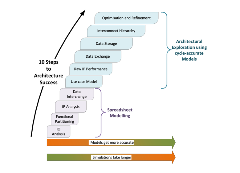
The shrinking of nodes means that chips are becoming ever more complex and require ever larger teams of engineers. To ensure that the design time of a chip does not increase as well, leading complexSoCdesigner, Sondrel, invests heavily into R&D to create novel modelling tools and flows to streamline the production of ASICs. Sondrel has codified this into its ten steps required to design an SoC architecture.
“This complexity means that companies are increasing outsourcing their SoCdesign to specialist companies such as ourselves who can deploy teams of multi-disciplinary engineers,” explained Graham Curren, Sondrel’s CEO. “Because Sondrel has created hundreds of ASICs across many application areas, we already have the experience in-house that ensure we can use the latest and best design techniques, many of which we have designed ourselves.”
Overall, the strategy forsuccessfully designing an SoC architectureis:-
- Break the problem into stages using a divide and conquer methodology
- As the level of detail increases at each stage, consider fewer options for exploration
- Use modelling to answer specific questions
- Focus resources as process progresses
- Avoid wasted simulation time
- Reduce data-set to be analysed
- Reduce simulation size and count to offset slow down
- Consider issues in a logical order to simplify cause and effect analysis, and to reduce iterations required
- Iterate to identify issues and fix before advancing to reduce wasted design effort.
- Balance thetrade-offof accuracy versus speed.

The 10 steps are: –
- Determines what the data is and what are the I/O constraints such as burstiness, latency, timing, and data formatting, to decide on the buffer requirements that is captured in a spreadsheet.
- Breaks the processing down into sub-tasks and groups parts of the SoC into common pieces of functionality.
- Identifies what third party IP blocks will be required to perform the steps of an algorithm and how much memory and compute power they require from their datasheets that can be fed into the modelling environment to give a more accurate representation of what all the IP blocks will be doing.
- Covers the method of exchanging data in between parts of an algorithm such as on-chip SRAM or external DDR memory as well as FIFO which are small spaces of memory on chip. The decision between SRAM and DDR depends on the size of the data and how often it needs to be accessed with large pieces of data going to external memory and small pieces of data to SRAM or FIFO.
- This is when a software representation is created of what the different stages are with the conceptual view of the algorithm and actual simulation objects that correspond to the different software stages of the algorithm. These require settings such as latency and processing cycles, and are joined by objects known as channels that indicate what the sequencing is.
- Having constructed all the simulation objects for the full algorithm, simulations can be run to see if the right sequencing of the algorithm has been captured.
- Uses models of the hardware platform with VPUs (Virtual Processor Units) that will run the software of step 5, each with its own local memory. Here the interface timing can be considered and communication domains defined with their assigned channels and evaluated. It also enables the configuration of the VPUs to be verified as correct.
- Takes the memory available to each VPU and remodels it as being connected to external memory via a common memory controller. This gives a more accurate representation of the connectivity of all the VPUs and memories in the final system.
- Adds the interconnect fabric. Instead of the direct connections between the VPUs and the memory controller, these are replaced by the interconnect fabric and the effects on the timing and performance evaluated. The interconnect fabric is then adjusted to meet the performance required, with previous stages being redone to achieve the required results.
- This is a good working model so, by simply adjusting settings, various simulations can be run to identify bottlenecks, what constraints there are in the system, and which parameters should be adjusted to improve the throughput and reduce the latency of the SoC. These take a few minutes to an hour to run so that it is straightforward and quick to test variants.
The first four steps can be done on paper or on a spreadsheet by calculation to understand the input/output dataflows into the SoC and what their characteristics are. The last six steps are simulation-based where software models are constructed and simulations run to generate results that inform about the system. An article covering this in more depth is available at www.sondrel.com/solutions/white-papers

