
According to latest research by Growth Market Reports, the global Semiconductor Electroplating Systems (Plating Equipment) market size reached USD 2.69 billion in 2025, with a robust growth trajectory supported by a CAGR of 7.4% from 2026 to 2034. This growth is primarily driven by the increasing adoption of advanced semiconductor devices and the surging demand for miniaturized electronic components across AI, automotive, and communications verticals. By 2034, the market is forecasted to attain a value of USD 5.11 billion, reflecting strong industry momentum and expanding applications across multiple end-use sectors.
The Semiconductor Electroplating Systems Market is becoming increasingly important as chip manufacturers pursue smaller features, higher interconnect density, and advanced packaging architectures. Electroplating, also known as electrochemical deposition, enables controlled metal deposition on semiconductor wafers and panels, supporting the fabrication of interconnects, bumps, pillars, through-silicon vias (TSVs), and redistribution layers (RDLs).
Advanced Packaging Drives Market Demand
Rising Use of Copper Plating
Copper remains a major material for semiconductor electroplating because of its electrical conductivity and suitability for interconnect applications. Equipment manufacturers are developing systems capable of supporting copper via filling, copper pillar formation, bumping, and RDL processing. These applications are becoming increasingly important as manufacturers seek greater interconnect density and improved electrical performance.
Expansion of Panel-Level Packaging
Panel-level packaging is emerging as another important opportunity. Larger processing surfaces can potentially improve manufacturing economics while supporting advanced packaging designs. Commercial electroplating platforms are being developed for large panels used in fan-out packaging, including processes involving pillars, bumps, and RDLs.
Technological Developments Reshaping the Industry
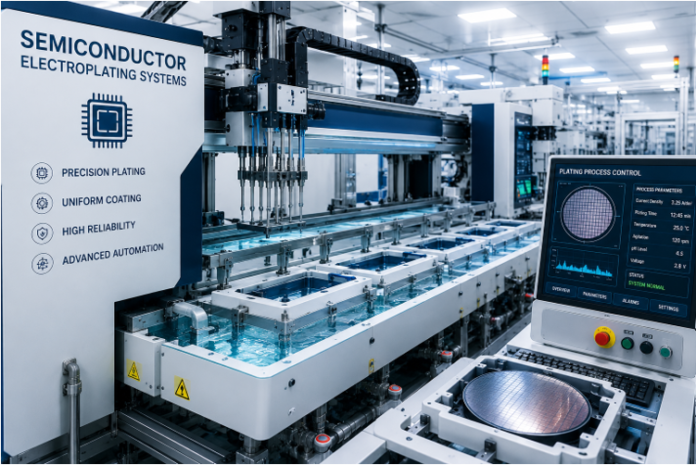
Manufacturers are focusing on horizontal plating architectures, improved fluid management, segmented anode control, pulse plating, and automated process monitoring. These technologies help improve deposition uniformity and address challenges associated with fine-pitch structures and high-aspect-ratio features. Recent research also highlights AI-enabled monitoring as an emerging approach for improving process control.
Automation is another major trend. Modern systems increasingly integrate wafer handling, chemical management, process controls, inspection, and data monitoring into automated production platforms. Such capabilities can help semiconductor manufacturers maintain consistent process conditions while reducing operator intervention and improving equipment utilization.
Key Market Opportunities
The expansion of artificial intelligence, high-performance computing, automotive electronics, 5G infrastructure, and advanced consumer devices is increasing demand for sophisticated semiconductor packages. These applications require faster data transfer, greater computing performance, and improved thermal and electrical characteristics, encouraging manufacturers to invest in advanced interconnect technologies.
Compound semiconductor manufacturing also represents a developing opportunity. Electroplating systems are being adapted for materials and applications involving silicon carbide, gallium nitride, and gallium arsenide, alongside metals such as copper, nickel, tin-silver, and gold.
Challenges Facing the Market
Despite strong opportunities, semiconductor electroplating requires exceptionally precise process control. Variations in current density, chemical concentration, temperature, fluid movement, and surface conditions can influence deposition quality. Maintaining consistent performance across wafers and panels therefore remains a major technical challenge.
Equipment developers must also address chemical consumption, contamination control, wastewater management, maintenance requirements, and increasingly stringent manufacturing standards. As semiconductor geometries become more sophisticated, achieving high throughput without compromising uniformity will remain a central industry challenge.
Competitive Landscape
Lam Research Corporation
Tokyo Electron Limited
Applied Materials Inc.
SCREEN Holdings Co., Ltd.
Shibaura Mechatronics Corporation
Semes Co., Ltd.
ULVAC, Inc.
SÜSS MicroTec SE
RENA Technologies GmbH
Technic Inc.
Future Outlook
The Semiconductor Electroplating Systems Market is positioned for sustained expansion through 2034 as semiconductor manufacturers increase their reliance on advanced interconnects and packaging technologies. Future systems are expected to emphasize automation, intelligent monitoring, higher throughput, precise deposition, and flexible processing for wafers and large-format panels. The equipment suppliers that successfully combine process precision, productivity, scalability, and advanced data-driven controls are likely to gain significant opportunities. The continued evolution of AI processors, chiplets, HBM, 3D integration, and heterogeneous packaging should further strengthen the strategic importance of semiconductor electroplating systems across the global semiconductor manufacturing ecosystem.

