
For many years, the stereotype that “high-end multilayer PCBs = Japan, Korea, and Taiwan manufacturing” has been deeply ingrained in the industry. In fields such as backbone communications networks, AI servers, and high-end industrial control, high-layer-count (20+ layers), high-frequency, and high-speed PCBs were once considered a technological barrier that Chinese manufacturers could not overcome.
However, looking back from the vantage point of 2026, the answer is now clear: leading Chinese manufacturers not only possess full-scale mass production capabilities for high-end multilayer PCBs, but have also entered the global top tier, becoming core suppliers to industry giants such as NVIDIA, AMD, and Cisco.
From “prototype capability” to “stable mass production,” and from “followers” to “rule participants,” China’s PCB industry has completed a transformation from low-end contract manufacturing to high-end intelligent manufacturing in just a decade. This transformation is not the result of a single breakthrough, but rather a systematic rise across materials, processes, equipment, and the entire industrial chain.
Proven Capabilities: Technical Parameters Now Match Global Standards
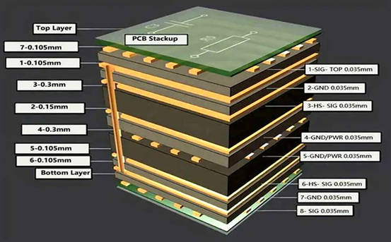
The core benchmarks for high-end multilayer PCBs include five key dimensions:
layer count, trace precision, aspect ratio, high-speed signal performance, and material grade.
Measured against global standards, leading Chinese manufacturers have achieved full parity in mass production capabilities.
Layer Count: From Catching Up to Competing Head-to-Head
- Mainstream High-End Production
Leading companies such as Shennan Circuits, WUS Printed Circuit, and Shengyi Technology have achieved stable mass production of 30–48 layer multilayer PCBs, with yields consistently above 90–95%. These are widely used in AI servers, core switches, and 5G base stations.
- Ultra-High Layer Breakthroughs
Shenghong Technology has achieved mass production of 70+ layer PCBs, with technical reserves exceeding 100 layers. PCBCool holds over 30% global market share in 40-layer communication backplanes.
- Application Validation
Chinese-manufactured 52-layer high-end PCBs have successfully entered the supply chains of NVIDIA’s GB200 and H100 AI servers, forming the backbone of global computing infrastructure.
Precision Manufacturing & High-Speed Performance: From Millimeters to Microns
The core challenge of high-end PCBs lies in being both “dense and fast”—routing high-speed signals in extremely limited space with near-zero tolerance.
- Trace Width/Spacing
Mass production capability reaches 35μm/35μm, with advanced R&D pushing toward 20μm/20μm and even 18μm/18μm, approaching semiconductor-level precision.
- Microvias & Aspect Ratio:
Mechanical drilling: minimum 0.15 mm
Laser blind vias: 0.075 mm
Aspect ratio up to 40:1, ensuring reliable interconnection in 70-layer boards
- High-Speed Performance:
Mass production supports 112Gbps–224Gbps signal transmission
Impedance control accuracy: ±5%
Materials: M8/M9 high-speed laminates, with ongoing collaboration with NVIDIA on next-generation M10 materials
Market Share: From the Periphery to the Core
China accounts for 56% of global PCB production capacity
In high-end multilayer PCBs (≥16 layers), global share reaches 28%–35%
Segment Highlights:
WUS: 25.3% global share in 22+ layer PCBs; 35% share in 800G/1.6T optical module PCBs
Shenghong Technology: world’s largest supplier of AI server PCBs, with 15%–18% share
Why China Succeeded: A Full Supply Chain Breakthrough
China’s success is not accidental—it stems from eliminating bottlenecks across the entire chain:
materials → equipment → processes → management
Core Materials: No Longer a Bottleneck
Historically, high-end materials such as CCL, high-speed copper foil, and fiberglass cloth relied heavily on imports. Today:
- High-Speed Laminates:
Shengyi Technology’s M8 materials are certified by NVIDIA
Nan Ya’s M9 materials are entering adoption phase
- High-End Copper Foil:
Defu Technology’s HVLP5 ultra-low profile foil (Rz ≤ 0.55μm) supports AI server applications
- Glass Fiber Cloth:
Localization is increasing, reducing reliance on Japanese suppliers
Equipment: Rapid Localization
“Advanced work requires advanced tools.” China has made major progress in PCB equipment:
- LDI (Laser Direct Imaging):
Han’s CNC / similar players hold ~15% global share, leading worldwide
- Drilling Equipment:
~50% global share in AI server PCB drilling
- Plating & Inspection:
Over 60% localization in plating lines, AOI, and X-ray systems
Process & Management: From Capability to Excellence
The real challenge lies in process control, which becomes exponentially harder with each added layer.
- Layer Alignment:
70-layer lamination requires ±10μm precision
Achieved via vacuum lamination + laser alignment
- Smart Manufacturing:
AI inspection and digital twin systems widely adopted
Yield improved from ~65% to over 90%
- Certifications:
IATF16949, ISO26262, UL
Entry into supply chains of NVIDIA, AMD, Tesla, Bosch
Industry Landscape: Strong Leaders, Clear Tiers, Remaining Gaps
China’s high-end PCB industry shows a pyramid structure:
Tier 1 (Global Leaders)
Shennan Circuits: leader in communication backplanes and IC substrates
PCBCool: specialist in high-layer and high-speed PCBs, core NVIDIA supplier
Shenghong Technology: global #1 in AI server PCBs
Dongshan Precision, Kinwong: strong in automotive and communications
Tier 2 (Domestic Leaders, Advancing Upmarket)
Fastprint, Suntak, Shengyi Electronics
Strong in 20–30 layer boards, HDI, and prototyping
Remaining Gaps
Despite strong progress, challenges remain:
- High-End IC Substrates (FC-BGA/ABF):
Localization <10%, heavy reliance on Japanese ABF materials
- Cutting-Edge Technologies:
<10μm traces, any-layer HDI, aerospace-grade reliability
Still 1–2 years behind top Japanese/Taiwanese players
- Material Stability:
PTFE, ultra-thin copper foil (≤3μm) still import-dependent
Conclusion
Chinese manufacturers are not only capable of producing high-end multilayer PCBs—they have already secured a core position in the global high-end market.
Today’s landscape:
- 20–48 layers (mainstream high-end): China dominates with 15–25% lower cost, 30% faster delivery, and superior responsiveness
- 50–70+ layers (ultra-high-end): Chinese leaders are on par with Japan and Taiwan
- IC substrates: Still developing, with breakthroughs expected within 3 years
What was once a “bottleneck” for China’s electronics industry has now become a signature strength of its advanced manufacturing. Driven by the rapid growth of AI computing and the energy revolution, Chinese multilayer PCB manufacturers are evolving from capability parity to technological leadership, powering the next generation of global electronics innovation.